LTC3446
16
3446ff
applicaTions inForMaTion
VLDO LINEAR REGULATOR DESIGN
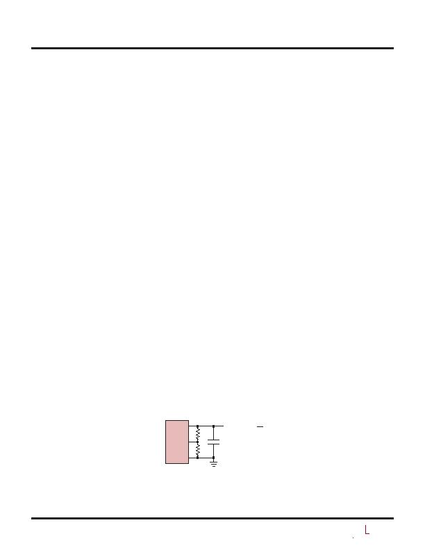
Adjustable Output Voltage
Each VLDO regulators output voltage is set by the ratio
of two external resistors as shown in Figure 2. The VLDO
regulator servos the output to maintain the LV
FB
pin voltage
at 0.4V (referenced to ground). Thus the current in R1 is
equal to 0.4V/R1. For good transient response, stability and
accuracy, the current in R1 should be at least 8礎, thus
the value of R1 should be no greater than 50k. The current
in R2 is the current in R1 plus the LV
FB
pin bias current.
Since the LV
FB
pin bias current is typically <10nA, it can
be ignored in the output voltage calculation. The output
voltage can be calculated using the formula in Figure 2.
Note that in shutdown, the output is turned off and the
divider current will be zero once C
OUT
is discharged.
Each VLDO regulator operates at a relatively high gain of
0.7礦/mA referred to its LV
FB
input. Thus a load current
change of 1mA to 300mA produces a 0.2mV drop at the
LV
FB
input. To calculate the change referred to the output,
simply multiply by the gain of the feedback network (i.e.,
1 + R2/R1). For example, to program the output for 1.2V,
choose R2/R1 = 2. In this example, an output current
change of 1mA to 300mA produces 0.2mV " (1 + 2) =
0.6mV drop at the output.
Because the LV
FB
pins are relatively high impedance (de-
pending on the resistor dividers used), stray capacitance
at these pins should be minimized (<10pF) to prevent
phase shift in the error amplifier loop. Additionally, special
attention should be given to any stray capacitances that
can couple external signals onto the LV
FB
pins producing
undesirable output ripple. For optimum performance,
connect each LV
FB
pin to its resistor divider with a short
PCB trace and minimize all other stray capacitance to the
LV
FB
pin.
VLDO Regulator Output Capacitance and Transient
Response
The VLDO regulators are designed to be stable with a
wide range of ceramic output capacitors. The ESR of the
output capacitor affects stability, most notably with small
capacitors. A minimum output capacitor of 1礔 with an
ESR of 0.05?or less is recommended to ensure stability.
The VLDO regulators are micropower devices and output
transient response will be a function of output capacitance.
Larger values of output capacitance decrease the peak
deviations and provide improved transient response for
larger load current changes. Note that bypass capacitors
used to decouple individual components powered by a
VLDO regulator will increase the effective output capaci-
tor value. High ESR tantalum and electrolytic capacitors
may be used, but a low ESR ceramic capacitor must be
in parallel at the output. There is no minimum ESR or
maximum capacitor size requirements.
Extra consideration must be given to the use of ceramic
capacitors. Ceramic capacitors are manufactured with a
variety of dielectrics, each with different behavior across
temperature and applied voltage. The most common di-
electrics used are Z5U, Y5V, X5R and X7R. The Z5U and
Y5V dielectrics are good for providing high capacitances
in a small package, but exhibit large voltage and tem-
perature coefficients as shown in Figures 3 and 4. When
used with a 2V regulator, a 1礔 Y5V capacitor can lose as
much as 75% of its intial capacitance over the operating
temperature range. The X5R and X7R dielectrics result
Figure 2. Programming a VLDO Regulators Output Voltage
R2
C
OUT
3446 F02
V
OUT
= 0.4V 1+
R2
R1
R1
( )
LV
OUT
LV
FB
GND
LTC3446
发布紧急采购,3分钟左右您将得到回复。
相关PDF资料
LTC3537EUD#TRPBF
IC REG DL BST/LINEAR SYNC 16-QFN
LTC3541EDD#TRPBF
IC REG DL BCK/LINEAR SYNC 10-DFN
LTC3670EDDB#TRPBF
IC REG TRPL BCK/LINEAR 12DFN
LTC3672BEDC-1#TRPBF
IC REG TRPL BCK/LINEAR 8-DFN
LTC3700EMS#TRPBF
IC REG DL BUCK/LINEAR 10MSOP
LTC4151HMS#TRPBF
IC PWR MONITOR MS 80V SD 10MSOP
LTC4210-2CS6#TRM
IC CONTROLLER HOT SWAP TSOT23-6
LTC4211IMS8
IC CONTROLLER HOT SWAP 8-MSOP
相关代理商/技术参数
LTC3446IDE#TRPBF
功能描述:IC REG TRPL BCK/LINEAR 14-DFN RoHS:是 类别:集成电路 (IC) >> PMIC - 稳压器 - 线性 + 切换式 系列:- 标准包装:2,500 系列:- 拓扑:降压(降压)同步(3),线性(LDO)(2) 功能:任何功能 输出数:5 频率 - 开关:300kHz 电压/电流 - 输出 1:控制器 电压/电流 - 输出 2:控制器 电压/电流 - 输出 3:控制器 带 LED 驱动器:无 带监控器:无 带序列发生器:是 电源电压:5.6 V ~ 24 V 工作温度:-40°C ~ 85°C 安装类型:* 封装/外壳:* 供应商设备封装:* 包装:*
LTC3446IDE-PBF
制造商:LINER 制造商全称:Linear Technology 功能描述:Monolithic Buck Regulator with Dual VLDO Regulators
LTC3446IDE-TRPBF
制造商:LINER 制造商全称:Linear Technology 功能描述:Monolithic Buck Regulator with Dual VLDO Regulators
LTC3447
制造商:LINER 制造商全称:Linear Technology 功能描述:I2C Controllable Buck Regulator in 3mm × 3mm DFN
LTC3447EDD
功能描述:IC REG BUCK SYNC ADJ 0.6A 10DFN RoHS:否 类别:集成电路 (IC) >> PMIC - 稳压器 - DC DC 开关稳压器 系列:- 标准包装:2,500 系列:- 类型:升压(升压) 输出类型:可调式 输出数:1 输出电压:1.24 V ~ 30 V 输入电压:1.5 V ~ 12 V PWM 型:电流模式,混合 频率 - 开关:600kHz 电流 - 输出:500mA 同步整流器:无 工作温度:-40°C ~ 85°C 安装类型:表面贴装 封装/外壳:8-SOIC(0.154",3.90mm 宽) 包装:带卷 (TR) 供应商设备封装:8-SOIC
LTC3447EDD#PBF
功能描述:IC REG BUCK SYNC ADJ 0.6A 10DFN RoHS:是 类别:集成电路 (IC) >> PMIC - 稳压器 - DC DC 开关稳压器 系列:- 标准包装:250 系列:- 类型:降压(降压) 输出类型:固定 输出数:1 输出电压:1.2V 输入电压:2.05 V ~ 6 V PWM 型:电压模式 频率 - 开关:2MHz 电流 - 输出:500mA 同步整流器:是 工作温度:-40°C ~ 85°C 安装类型:表面贴装 封装/外壳:6-UFDFN 包装:带卷 (TR) 供应商设备封装:6-SON(1.45x1) 产品目录页面:1032 (CN2011-ZH PDF) 其它名称:296-25628-2
LTC3447EDD#TR
制造商:Linear Technology 功能描述:Conv DC-DC Single Step Down 2.5V to 5.5V 10-Pin DFN EP T/R
LTC3447EDD#TRPBF
功能描述:IC REG BUCK SYNC ADJ 0.6A 10DFN RoHS:是 类别:集成电路 (IC) >> PMIC - 稳压器 - DC DC 开关稳压器 系列:- 标准包装:2,500 系列:- 类型:升压(升压) 输出类型:可调式 输出数:1 输出电压:1.24 V ~ 30 V 输入电压:1.5 V ~ 12 V PWM 型:电流模式,混合 频率 - 开关:600kHz 电流 - 输出:500mA 同步整流器:无 工作温度:-40°C ~ 85°C 安装类型:表面贴装 封装/外壳:8-SOIC(0.154",3.90mm 宽) 包装:带卷 (TR) 供应商设备封装:8-SOIC